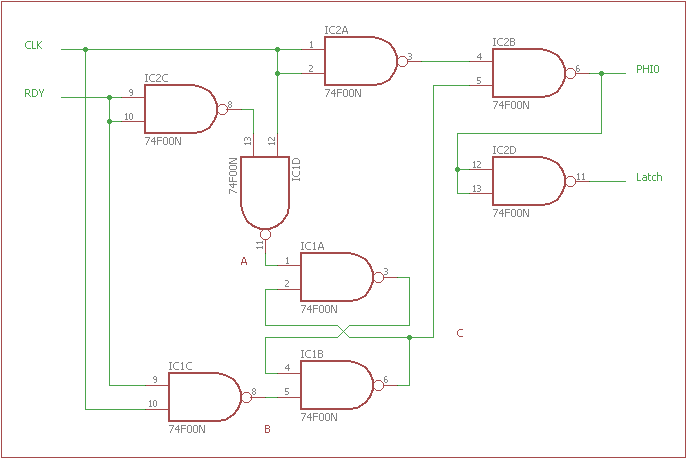
Hi Ruud,

What you have basically coded up into the GAL is a series of NAND gates and you are using some of the internal feedback paths (from
outputs to inputs) to "fake" a set/reset flip-flop. But what happens when you apply power? Will FF1 or FF2 be set?

Depending upon the GAL you are using - it may contain different types of flip-flops in the output logic macro cell (OLMC). For a V750C
that I have been using recently, I have used flip-flops with:

A clock input (.CK)
A D input (.D)
A Synchronous Preset (.SP)
An Asynchronous Reset (.AR)
An Output Enable (.OE)
And a Q and !Q output (which can also be used as a feedback).

From what you are saying about pin 1 being the clock - it seems as though you are using a relatively simple GAL where all configured flip-
flops would have the same clock.

You should have a look at the technical manual for the GAL you are using to see what options you have available for the OLMC flip-flop and
redesign your schematic around that.

I have just looked up the technical manual for the 16V8 GAL and indeed it has a single clock for each and every internal configured flip
flop wired to Pin 1 and a D input with a Q and !Q output with an Output Enable. Pin 11 is also dedicated to the Output Enable function in
this case. The Q output from each flip-flop will be set LOW when power is applied to the GAL.

I have copied and pasted a section from my fairly complex GAL into here so you can hopefully see the syntax of using a flip-flop with
WinCupl:

Pin 14 = RR;           /* Result register */

/* Logic Unit */
/* ========== */

RR.AR = RST;
RR.SP = LO;
RR.CK = I4_REG & !I3_REG & X1; /* Rising edge when opcode is in range 10000 to 10111 */

RR.D = (  ( RR           ) & Ix:OPCODE_NOP0 ) #
       (  ( LU_A         ) & Ix:OPCODE_LD   ) #
       (  (!LU_A         ) & Ix:OPCODE_LDC  ) #
       (  ( RR   &  LU_A ) & Ix:OPCODE_AND  ) #
       (  ( RR   & !LU_A ) & Ix:OPCODE_ANDC ) #
       (  ( RR   #  LU_A ) & Ix:OPCODE_OR   ) #
       (  ( RR   # !LU_A ) & Ix:OPCODE_ORC  ) #
       ( !( RR   $  LU_A ) & Ix:OPCODE_XNOR ) ;

DOUT = ( RR & Ix:OPCODE_STO ) #
       (!RR & Ix:OPCODE_STOC) ;

Hope this is good enough as a starter?

Regards,

Dave

> Message Received: Apr 18 2013, 08:14 AM
> From: "Baltissen, GJPAA (Ruud)" <ruud.baltissen@apg.nl>
> To: "'cbm-hackers@musoftware.de'" <cbm-hackers@musoftware.de>
> Cc:
> Subject: Help with GAL needed
>
> Hallo allemaal,
>
>
> I have programmed several GALs so far but they all contained only lineair equations. I have designed a WAIT circuit for the 65816, which
works fine, that is built using TTL gates: http://www.baltissen.org/images/65816rdy.png
> As you can see, this schematic contains a flipflop. I use the 'old' CUPL.EXE to compile my equations. Please have a look at my equations
for this schematic:
>
>
> 	Name		ISA bus with 65816, GAL #3b;
> 	Device	G16V8AS;
> 	Designer	Ruud Baltissen;
> 	Date		2013-04-18;
> 	Revision	V0.1;
>
> 	Assembly	--;
> 	Company 	--;
> 	Location	--;
> 	Partno 	--;
>
>
> /* Define Logic Operators */
> 	/* AND = &  */
> 	/* OR = #   */
> 	/* NOT = !  */
>
>
> /* Define Input Pins */
> 	pin  2 = CLK;
> 	pin  3 = RDY;
>
> /* Define Output Pins */
> 	pin 12 = PHI0;		/* regulated CLK */
> 	pin 13 = FF1;
> 	pin 14 = FF2;
>
> /* Boolean Equations */
> 	FF1  = !(!(!RDY & CLK) & FF2);
> 	FF2  = !(!(RDY & CLK) & FF1);
> 	PHI0 = !(!CLK & FF2);
>
>
> CUPL compiled without any problem. But does it mean the above is good? I know it can be optimised/simplified, but as you can see the
equations are a literally translation of the hardware. One part can be replaced by a single OR gate but then I would need at least three
ICs in real life, now only two.
>
> As you can see I reserved output pins for the flipflop. IMHO it cannot be done in another way. But I hope to be wrong in this case; the
less output pins I need, the better.
>
> Then there is the CLK input at pin 1. IMHO you only need it if you program (a part of) the GAL as counter. I know I haven't used any of
the internal registers, but I don't know what CUPL made of it. So I'm not sure yet if it is needed.
>
> Any help, suggestion, etc. is surely appreciated!
>
>
> --
>      ___
>     / __|__
>    / /  |_/     Groetjes, Ruud
>    \ \__|_\
>     \___|       http://www.baltissen.org
>
>
>
> De informatie in dit e-mailbericht is vertrouwelijk en uitsluitend bestemd voor de
> geadresseerde. Wanneer u dit bericht per abuis ontvangt, verzoeken wij u contact op te
> nemen met de afzender per kerende e-mail. Verder verzoeken wij u in dat geval dit
> e-mailbericht te vernietigen en de inhoud ervan aan niemand openbaar te maken.
> Wij aanvaarden geen aansprakelijkheid voor onjuiste, onvolledige dan wel ontijdige
> overbrenging van de inhoud van een verzonden e-mailbericht, noch voor daarbij
> overgebrachte virussen.
>
> APG Algemene Pensioen Groep NV is gevestigd te Heerlen en is ingeschreven in het
> handelsregister van de Kamer van Koophandel Limburg onder nummer 14099617
>
>
> The information contained in this e-mail is confidential and may be privileged.
> It may be read, copied and used only by the intended recipient.
> If you have received it in error, please contact the sender immediately by
> return e-mail; please delete in this case the e-mail and do not disclose its
> contents to any person. We don't accept liability for any errors, omissions,
> delays of receipt or viruses in the contents of this message which arise as a
> result of e-mail transmission.
>
> APG Algemene Pensioen Groep NV is registered in the trade register of the Chamber
> of Commerce Limburg, The Netherlands, registration number: 14099617
>
>
>        Message was sent through the cbm-hackers mailing list
>

       Message was sent through the cbm-hackers mailing list
Received on 2013-04-18 13:04:59
Archive generated by hypermail 2.2.0.