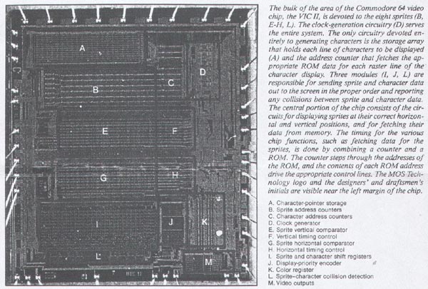
>>>> I've looked at the Y decoder on the 6561 (PAL) chip.
>>>
>>> Sorry if I didn't follow the discussion, but what does "look" mean?
>>
>> Look at this:
>> http://visual6502.org/images/pages/MOS_6561_VIC_die_shots.html
>>
>> (I don't make the pictures, I just look at them, fwiw).
>
> Still, looking at a die shot and being able to find out what the
> structures mean is not an easy thing... Is there a die shot of a
> VIC that tells you what the different parts are?

There is this one: http://www.mayhem64.co.uk/c64design2.jpg

It's not completely correct, and it leaves out all of the fun details.
Much too small for more details of course, but maybe it gives you an
idea.

When figuring out a chip, I usually start with the address and data
busses, from there the internal registers, and then the various clocks
(there are 12 clock signals on the VIC-II! -- 1, 2, 4, 8MHz, each two
phases, and colour clock, four phases).  It's depletion load NMOS, which
is quite easy to read once you get used to it (and have good
pictures :-) );
but almost every chip gives you some new structures (to keep it
interesting),
e.g. the VIC-II has bootstrapped clock gates (lots of them) and of
course
the various analog stuff.


Segher


       Message was sent through the cbm-hackers mailing list
Received on 2011-08-27 23:00:27
Archive generated by hypermail 2.2.0.