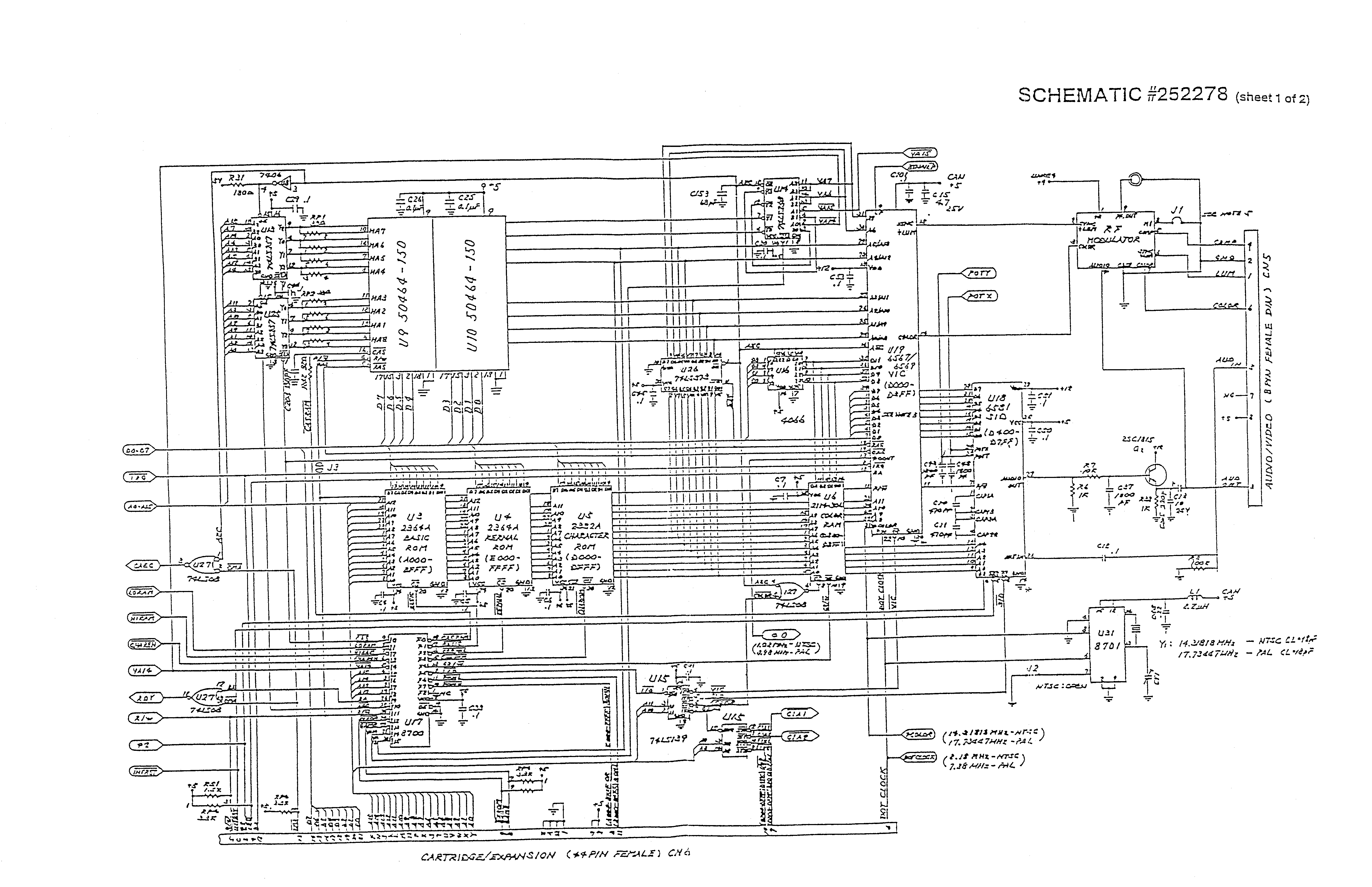
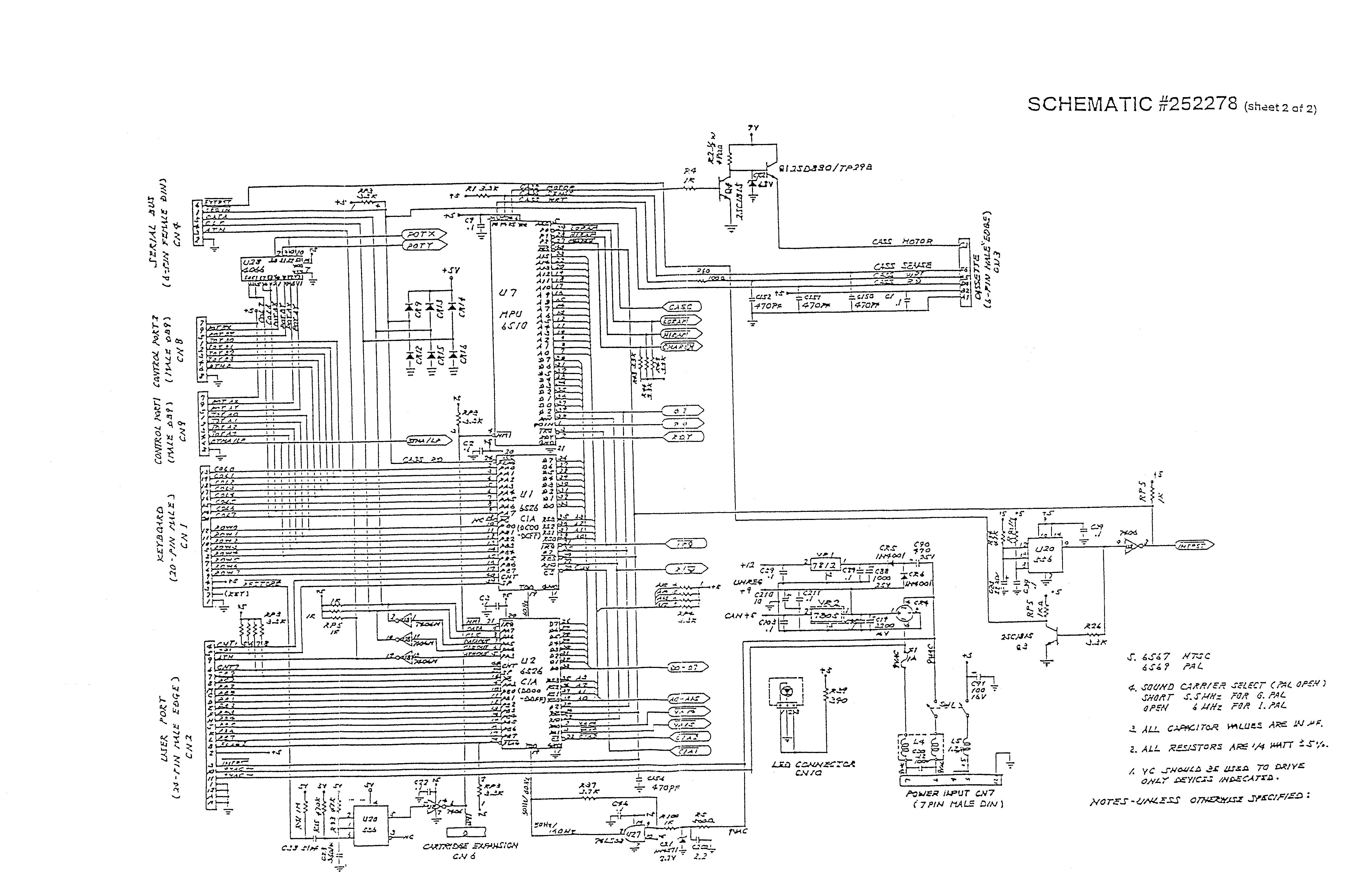
On 7/7/19 9:43 PM, Jim Brain wrote:
> Memory in a 250466 PCB went flaky, so I tried my hand at repair.  The
> PCB is the 3 ROM version, but with 4164 DRAMs.  After desoldering the
> DRAMs, socketing, and installing some new DRAMs (all working now), I
> decided to see if I could switch the unit over to SRAM.  It appears I
> and some other folks had similar ideas, as I see another project on
> Facebook to convert as well.  I went a different direction and leveraged
> a small CPLD to do the conversion.

That's a bit Overkill, you need just 2 TTLs to make it work. A 74HCT573
and a 74LS32 or 74LS04 (*) will do the trick.

(*) You need to either OR /RAS and /CAS to create the /CS for the RAM or
use both CS-Lines on a 128 KB SRAM and invert one signal since one of
them is high active.


> I decided to play around with the unit and map out the address pins.
> Interestingly, I find that MA6 and MA0 appear to be swapped on the PCB.
> I verified that MA6 indeed goes to MA0 on the 6567, though without a
> schematic, it's hard to trace MA6 (it goes through a '257, etc.).
> Anyone have a schematic? (Zimmers does not appear to have one)

Sure it does:

http://www.zimmers.net/anonftp/pub/cbm/schematics/computers/c64/252278-1.gif

http://www.zimmers.net/anonftp/pub/cbm/schematics/computers/c64/252278-2.gif

  Gerrit
Received on 2020-05-29 22:35:51
Archive generated by hypermail 2.3.0.