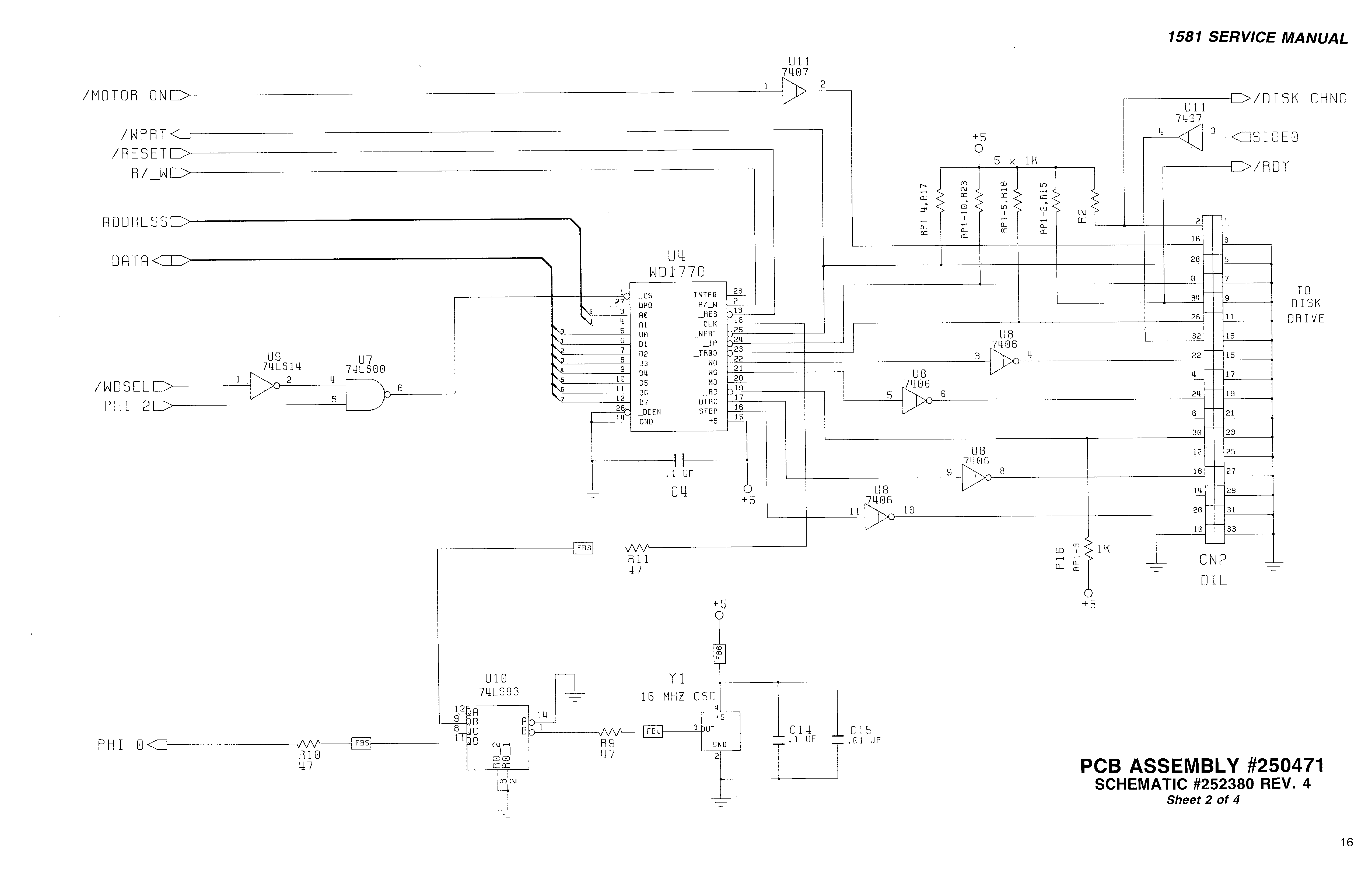
Hello,

* On Fri, Mar 11, 2022 at 07:06:46PM +0100 Francesco Messineo wrote:
> Hi,
>
> On Fri, Mar 11, 2022 at 6:13 PM Spiro Trikaliotis
> <ml-cbmhackers_at_trikaliotis.net> wrote:
> >
> > Hello,
> >
> > I am trying to understand the sources of the 1571 and 1581 drives.
> >
> > In the original drive sources of the 1571 and 1581 (as found on
> > zimmers.net), there is a macro WDTEST:
> >
> > WDTEST  .macro
> >         .ife <*!.$03
> >         nop
> >         .endif
> >         .endm
> >
> > I am not completely familiar with the syntax of the assembler used, but
> > if I understand it correctly, it issues a NOP if bit 0 and bit 1 of the
> > PC are both 0 - that is, the PC address is divisble by 4.
>
> wild guess:
> The WD1770 in the Commodore 1571 (and I guess in the 1581 too, but
> I've never seen one) has its chip select line
> qualified with the wrong clock. Let me explain better: when a
> peripheral device must be connected to the 6502's bus, it either has a
> phi2 input

According to the schematics, it is wired with PHI2:
http://www.zimmers.net/anonftp/pub/cbm/schematics/drives/new/1581/1581-16.gif

> Now, if one uses phi1 as "poor man's" inverted phi2, it turns out that
> the chip select to the WD1770 might happen too early (phi2 not yet
> high) and cause unpredictable
> behaviour.

Yes, this was part of my wild guess, too, that the timing is not
correct. The WD177x was not desinged with the 65xx family in mind.

> Since also the WD1770 need two address lines and they are supplied by
> A0 and A1, it was probably wise to never have both A0 and A1 both low
> just before a real access
> to this device, since its chip select has the wrong timing and maybe
> A0=A1=0 was the worst possible fake access to this device.

Well, in fact, it filters out the case when there are A1=1, A0=0 before
/CS going active. The next step after /CS going inactive would be A1=1,
A0=1 (it might be the release of /CS that is critical?)

I mean, A0=A1=1 is the DATA address. Here, a simple read let's the
WD177x decide that the data was read, and the signaling is removed.
That's why I believe this case might be the critical one.

Regards,
Spiro

--
Spiro R. Trikaliotis
https://spiro.trikaliotis.net/
Received on 2022-03-12 11:03:47
Archive generated by hypermail 2.3.0.