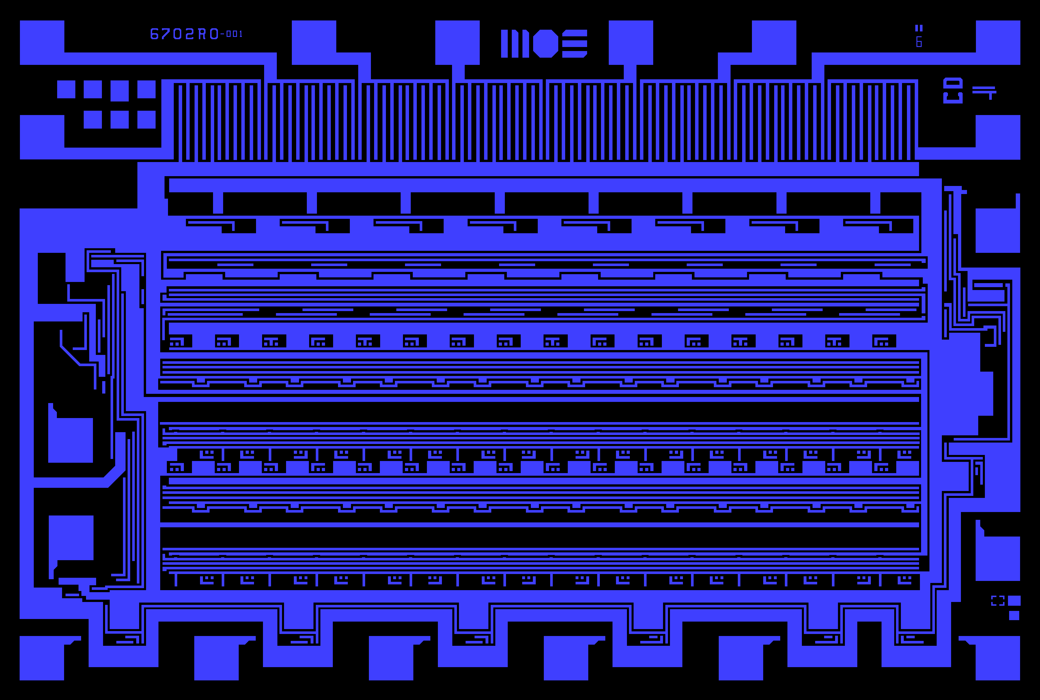
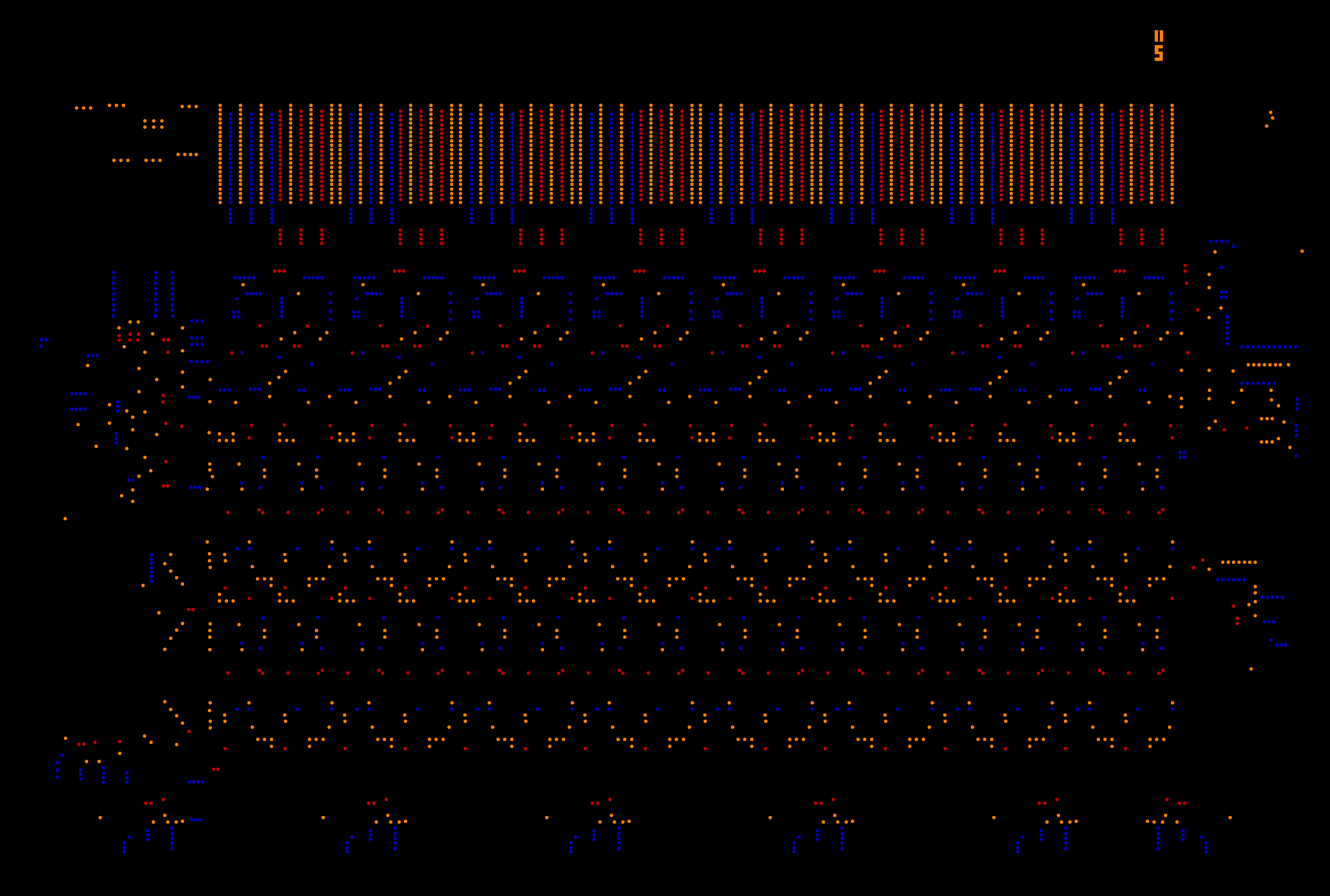
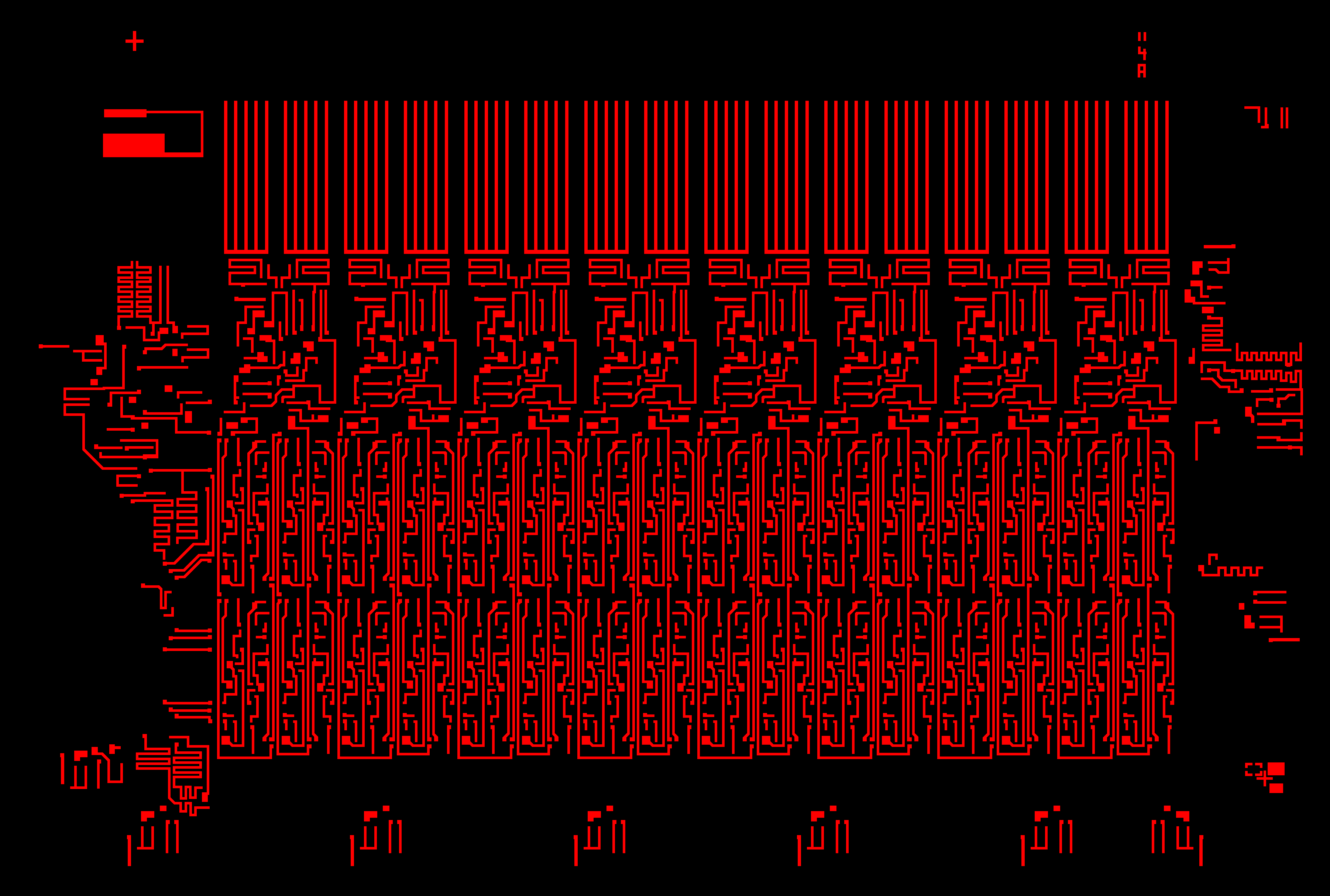
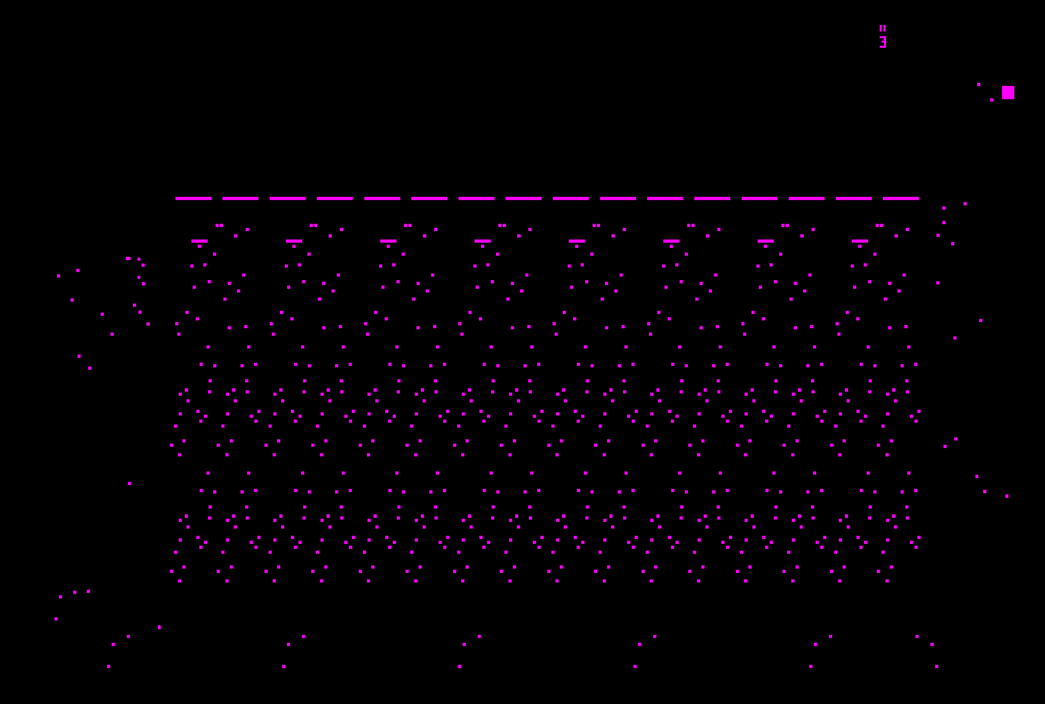
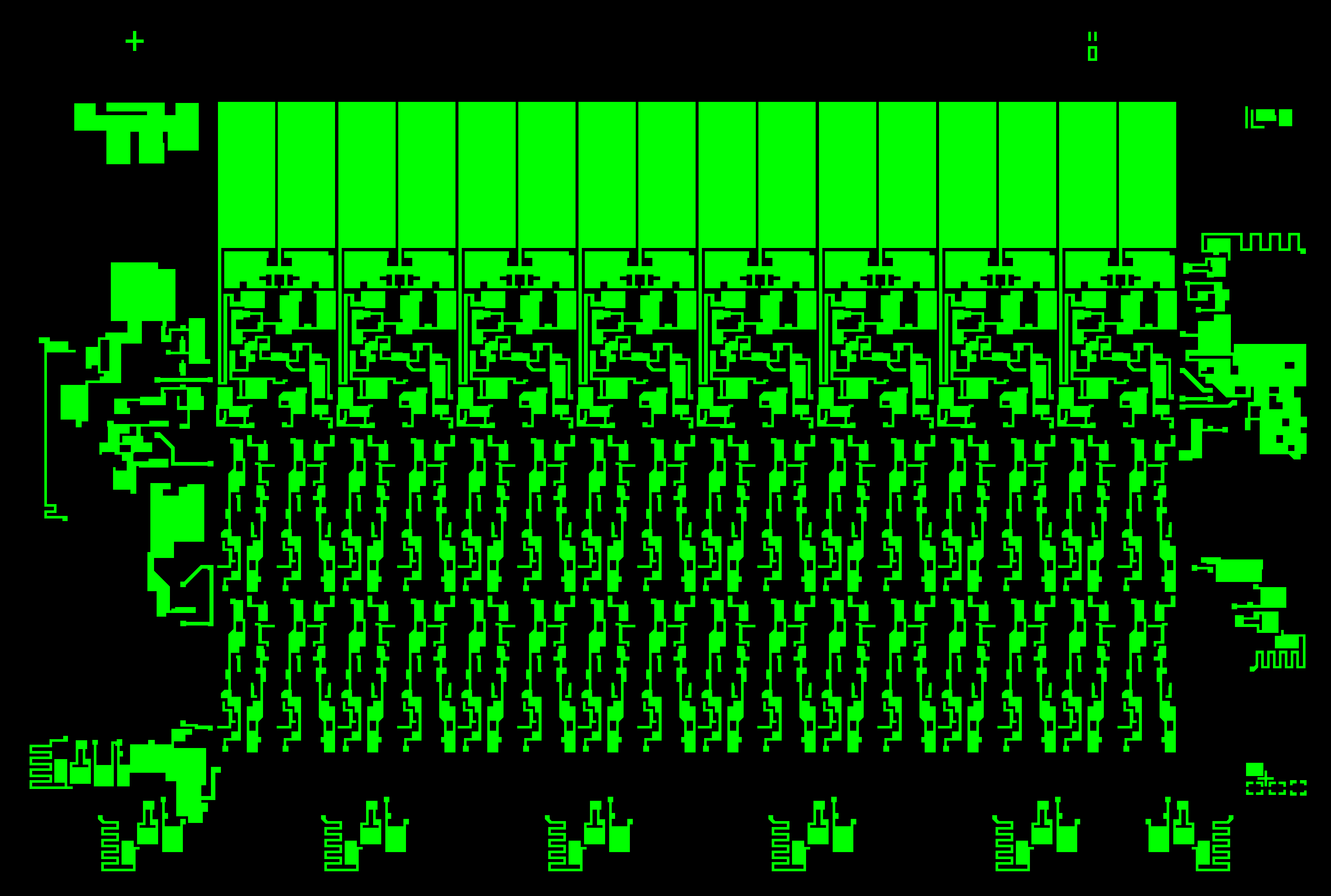
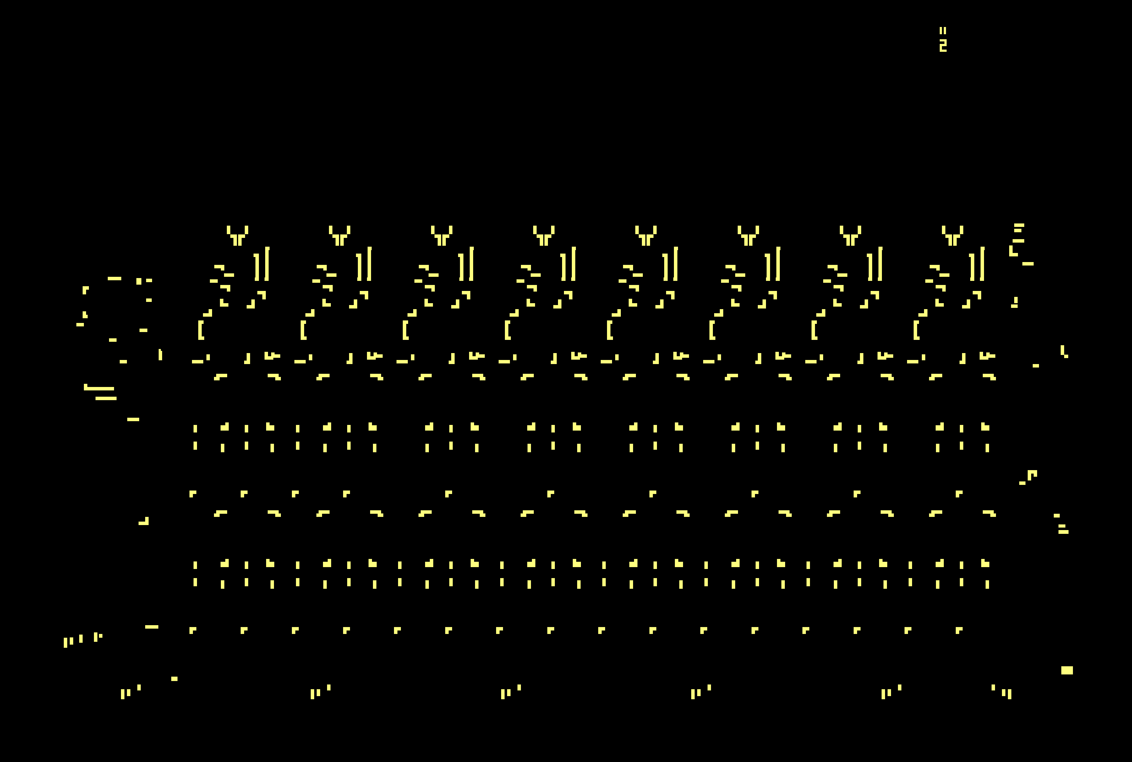
Hello.

I've drawn layers of 6702 based on die shot published on visual6502. As the
chip was not delayered yet the diffusion and buried contact layers are
sometimes only guesses as they are not visible when hidden below the metal
layer. Anyways I succeded in simulation of the chip and the results were
exactly what expected for repetitive inputs 00-01, 00-03 and 00-81 (hexa). I
did not test the other sequences because I suppose that they are OK. Maybe
if someone here has some more elaborate (not repeating) sequence for me to
test I'll test it.

If no one else wants to do that I can draw the schematic of the chip and do
some analysis. The chip itself looks quite simply, it consists of 1249
transistors.
Below is the copy of my posting to visual6502 forum - if you try to run my
simulator don't panic, it's quite slow, it runs for several minutes (some
85s on my i7):

=============================================================================

Hello.

I was thinking if this chip is easy and repetitive enough that diffusion and
buried layers could be renostructed just by thinking and intuition. I
couldn't resist and I drew it and simulated it.

Total: http://www.pastraiser.com/pictures/6702/6702_total.png
Metal: http://www.pastraiser.com/pictures/6702/6702_metal.png
Vias: http://www.pastraiser.com/pictures/6702/6702_vias.png
Colored vias: http://www.pastraiser.com/pictures/6702/6702_vias_colored.png
(suitable for analysis and schematic drawing)
Polysilicon: http://www.pastraiser.com/pictures/6702/6702_polysilicon.png
Buried contacts: http://www.pastraiser.com/pictures/6702/6702_buried.png
Diffusion: http://www.pastraiser.com/pictures/6702/6702_diffusion.png
Ion implants: http://www.pastraiser.com/pictures/6702/6702_ion.png (as my
simulator does not use it it is unverified).

Simulator: http://www.pastraiser.com/pictures/6702/Simulator.zip
Simulator is based on my 8085 simulator.
Simulator contains layers without test pictures (to get rid of its warnings)
and source code and executable (compiled as 64-bit application in visual c++
2012). It could be run as:
6702_Simulator 6702 >Test_01.txt
The text file Test_01.txt is in the archive as well it contains simulation
for periodic inputs 00 (even input) and 01 (odd input). The simulated chip
outputs corresponds with values published here:
http://cbm-hackers.2304266.n4.nabble.com/6702-chip-td4622550.html in comment
from user Rhialto May 11, 2012; 9:58am. I tried as well values 00-03 and
00-81 (hexa) and the result was as described.

From quick view observation - as discussed in CBM hackers list - for each
data bit (D0-D7) there is an 8-bit shift register which can be modified to
any length shorter than this by simply modifying the metal layer (there are
three metal options for each stage).
As I said - diffusion and buried layer are more or less guesses because as
they are behind the metal they are rather invisible. Ion layer is completely
my guess.
If someone wants to draw schematics or simulate it more - just go ahead.

Pavel


       Message was sent through the cbm-hackers mailing list
Received on 2013-02-22 01:31:14
Archive generated by hypermail 2.2.0.